What is Photolithography? An In-depth Explanation
Photolithography is a process that has transformed various industries, from semiconductors to biotechnology, in unprecedented ways. It is a method of transferring a pattern onto a substrate, such as a silicon wafer, using light and a series of chemical processes. In this article, we will explore the history, key concepts, applications, current trends, and future directions of photolithography. We will also provide case studies and examples to illustrate its practical applications.
Historical Context
The history of photolithography can be traced back to the 1820s when Joseph Nicéphore Niépce created the first photograph. However, it was not until the 1950s that photolithography began to be widely used in the semiconductor industry. This was driven by the need to create smaller, more powerful transistors that could be integrated into microchips.
In 1958, Jack Kilby and Robert Noyce independently developed the integrated circuit, a crucial breakthrough that paved the way for the modern semiconductor industry. Photolithography became an essential tool for creating these circuits, enabling manufacturers to create intricate patterns on a silicon wafer with incredible precision.
Since then, photolithography has continued to evolve, becoming more sophisticated and versatile. It is now used in a wide range of applications, from creating microprocessors to printing microfluidic devices for biomedical research.
Photolithography Concepts and Principles
At its core, photolithography involves a series of steps that allow patterns to be transferred onto a substrate. These steps include:
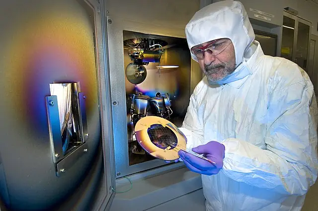
- Substrate preparation: The substrate, such as a silicon wafer, is cleaned and prepared to ensure that it is free of contaminants that could interfere with the photolithography process
- Photoresist coating: A photoresist, a light-sensitive material, is coated onto the substrate. The photoresist can be either positive or negative, depending on whether the pattern is created by exposing the areas that will be removed or by exposing the areas that will remain.
- Exposure: A mask, which contains the desired pattern, is placed on top of the photoresist-coated substrate. The substrate is then exposed to light, typically using a UV source. The light passes through the mask and selectively exposes the photoresist.
- Development: The photoresist is then developed, using a series of chemicals, to remove the areas that were exposed to light. This creates the desired pattern on the substrate.
- Etching: If the substrate is not the final product, an etching process may be used to remove the substrate material that is not protected by the photoresist.
- Stripping: The remaining photoresist is removed from the substrate, leaving behind the desired pattern.
Applications of Photolithography
Photolithography has a wide range of applications across various industries, from semiconductor manufacturing to biotechnology. Here are some of the key applications of photolithography:
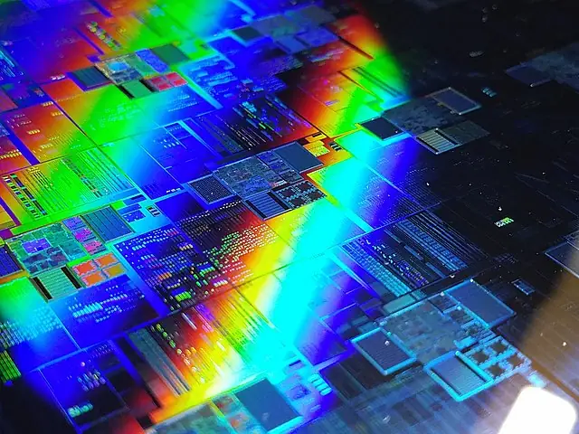
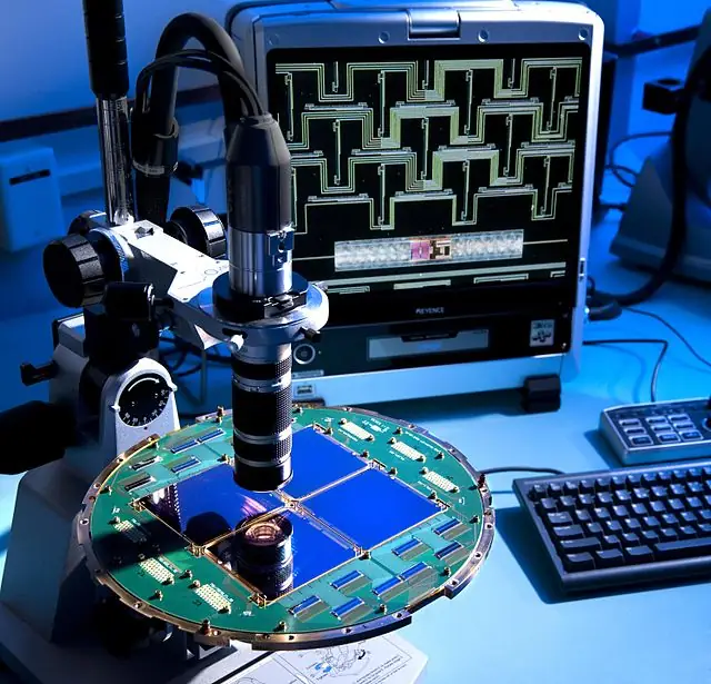
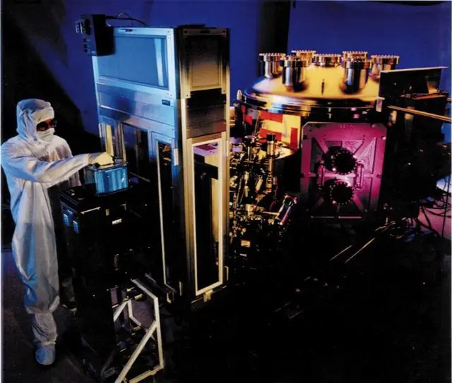
- Semiconductor manufacturing: Photolithography is essential for creating microchips, which are used in a wide range of electronic devices, such as computers, smartphones, and televisions. The precise patterns created by photolithography enable manufacturers to create smaller and more powerful microchips, leading to faster and more efficient electronic devices.
- Biotechnology: Photolithography is used to create microfluidic devices, which are used in biomedical research and diagnostics. These devices allow researchers to manipulate tiny amounts of fluids and perform complex experiments on a microscopic scale. Photolithography is also used to create microarrays, which are used to analyze gene expression and detect diseases.
- Optics: Photolithography is used to create micro-optics, such as lenses and gratings, with incredibly high precision. These optics are used in a wide range of applications, such as telescopes, cameras, and laser systems.
- Display industry: Photolithography is used to create the patterned layers in displays, such as OLED and LCD screens. This allows manufacturers to create displays with better color reproduction, higher contrast, and lower power consumption.
- Printed circuit boards: Photolithography is used to create the circuit patterns on printed circuit boards, allowing them to be more compact and efficient. This has led to the development of smaller and more powerful electronic devices, such as smartphones and tablets.
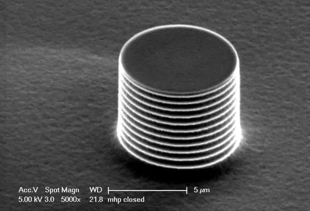
- Nanotechnology: Photolithography is used in the development of nanoscale materials and devices, such as quantum dots and nanowires. These materials have unique electronic and mechanical properties that make them suitable for a wide range of applications, such as solar cells, sensors, and batteries.
- MEMS: Photolithography is used in the development of micro-electromechanical systems (MEMS), which are tiny devices that combine mechanical and electronic components. MEMS are used in a wide range of applications, such as accelerometers, gyroscopes, and pressure sensors.
- Photonics: Photolithography is used to create photonic devices, such as waveguides and couplers, which are used in optical communication systems. These devices enable high-speed data transfer and communication over long distances.
Overall, photolithography is a crucial tool for creating precise patterns on a wide range of substrates. Its versatility and precision have enabled it to transform various industries and drive innovation in electronics, biotechnology, optics, and other fields.
Current Trends and Future Directions For Photolithography
Recent breakthroughs in photolithography have focused on improving its resolution, throughput, and versatility. One of the most significant trends in photolithography is the development of new types of photoresists that can be used with different wavelengths of light. This has enabled manufacturers to create smaller patterns with higher precision, leading to the development of new types of microchips and sensors.
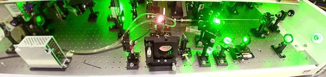
Another trend is the use of alternative sources of light, such as extreme ultraviolet (EUV) light, which has a shorter wavelength than traditional UV light. EUV lithography is expected to become increasingly important as manufacturers continue to push the limits of pattern size and density. However, EUV lithography has some technical challenges, such as the need for specialized optics and materials that can withstand the high-energy light.
Another promising development is the use of machine learning algorithms to optimize photolithography processes. These algorithms can analyze large amounts of data and identify patterns that are difficult for humans to detect. This has the potential to improve the accuracy and efficiency of photolithography, leading to faster production times and lower costs.
In the future, photolithography is expected to continue to play a vital role in a wide range of industries. One area of growth is the use of photolithography in 3D printing, allowing manufacturers to create complex 3D structures with high precision. Another area of potential growth is the use of photolithography in the development of new materials, such as graphene and other 2D materials, which have unique electronic and mechanical properties.
Limitations and Challenges
While photolithography has many advantages, there are also some limitations and challenges associated with its use. One of the primary limitations is the difficulty of creating complex patterns on non-planar surfaces, such as spheres or curved surfaces. This has limited the use of photolithography in certain applications, such as creating micro-optics with curved surfaces.
Challenges include improving the speed and efficiency of photolithography, reducing the cost of equipment and materials, and developing new types of photoresists that can withstand high-energy light. These challenges will require continued innovation and collaboration between researchers and manufacturers.
Conclusion
In conclusion, photolithography is a powerful tool that has revolutionized various industries, from semiconductors to biotechnology. It allows manufacturers to create intricate patterns on a substrate with incredible precision, enabling the development of smaller, more powerful devices. The process has continued to evolve, becoming more sophisticated and versatile, and has led to the development of new types of microchips, sensors, displays, and materials.
While there are some ethical concerns, limitations, and challenges associated with photolithography, its potential benefits cannot be overstated. As the technology continues to evolve, it will likely play an increasingly vital role in a wide range of industries, from healthcare to energy.
By understanding the history, key concepts, applications, current trends, and future directions of photolithography, we can appreciate the significance of this technology and its impact on society. Whether you are a researcher, engineer, or simply someone interested in science and technology, photolithography is a topic that is well worth exploring further.