Wafer-Scale Nanofabrication of Telecom Single-Photon Emitters
Researchers from the Helmholtz-Zentrum Dresden-Rossendorf (HZDR) have made a significant breakthrough in wafer-scale nanofabrication, enabling the creation of controllable single-photon emitters in silicon for photonic quantum technologies.
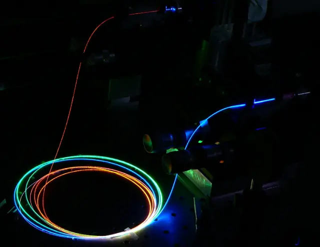
Photonic integrated circuits (PICs) have become increasingly important in the field of quantum photonics experiments. These circuits use photons, rather than electrons, to provide functions for information signals, typically in the near-infrared spectrum. With many integrated photonic components, PICs can generate, route, process, and detect light on a single chip.
The integration of single-photon sources in a controllable way is necessary to implement millions of photonic qubits in PICs. To run quantum computation protocols, these photons must be indistinguishable. With this, industrial-scale photonic quantum processor production would become feasible. However, the currently established fabrication method is not compatible with today’s semiconductor technology.
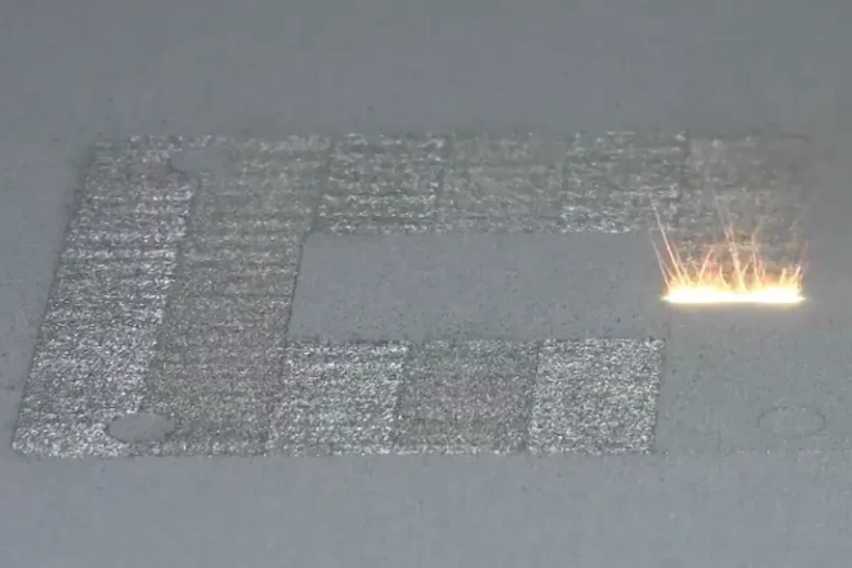
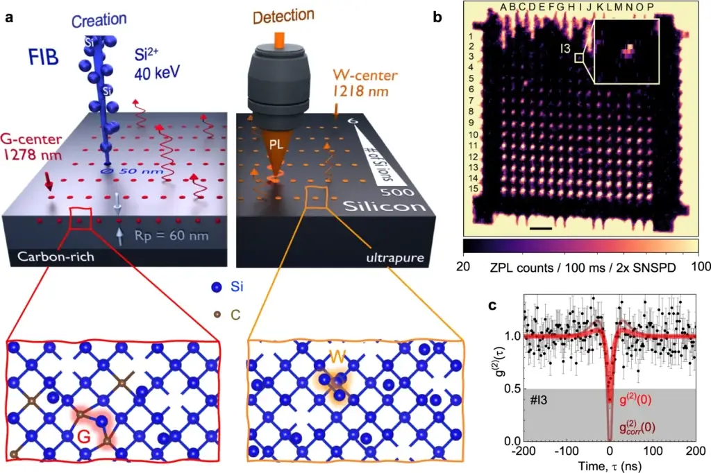
The HZDR researchers previously generated single photons on a silicon wafer, but only in a random and non-scalable way. However, they have now made a significant breakthrough by using focused ion beams from liquid metal alloy ion sources to place single-photon emitters at desired positions on the wafer while obtaining a high creation yield and high spectral quality.
Furthermore, the single-photon emitters were subjected to a rigorous material testing program, with no degradation of their optical properties observed after several cooling-down and warming-up cycles. These findings meet the preconditions required for mass production later on.
Using both methods, the team can create dozens of telecom single-photon emitters at predefined locations with a spatial accuracy of about 50 nm. They emit in the strategically important telecommunication O-band and exhibit stable operation over days under continuous-wave excitation.
“This work really allowed us to take advantage of the state-of-the-art silicon processing cleanroom and electron beam lithography machines at the Nano Fabrication facility Rossendorf,” explains Dr. Ciarán Fowley, Cleanroom group leader and Head of Nanofabrication and Analysis.
The realization of controllable fabrication of single-photon emitters in silicon is a highly promising development for photonic quantum technologies. It enables the creation of millions of photonic qubits in PICs and opens up the possibility of an efficient and scalable production of photonic quantum processors. With the technological readiness of these single-photon emitters for mass production in semiconductor fabs, the future of photonic quantum technologies is bright.
The findings are published in the journal Nature Communications.