Compact Photonic Chip System Brings Miniaturized Atomic Clocks Closer to Reality
Researchers have developed a groundbreaking compact photonic chip system that paves the way for miniaturized strontium atomic clocks. The achievement has significant implications for atomic technologies, as miniaturization could lead to a range of benefits in applications such as GPS and communication systems.
Background on Atomic Clocks and Optical Systems
Atomic clocks are at the core of various applications, including timekeeping, navigation, and telecommunications, as they offer exceptional precision and stability in measuring time. These sophisticated devices exploit the regular vibrations of atoms, such as cesium or strontium, to produce highly accurate and stable time signals. Due to their unparalleled precision, atomic clocks have become indispensable in numerous fields, including global positioning systems (GPS), communication networks, financial services, and scientific research.
In atomic clocks, optical systems are responsible for controlling the laser beams that interact with the atoms. The performance of these clocks relies on precise control of wavelength, power, and polarization of coherent free-space light to address the optical transitions in atomic systems. Achieving this level of control is feasible with laboratory-scale setups; however, when scaling down these optical systems for commercialization, several challenges arise.
One of the primary obstacles in miniaturizing optical systems is maintaining the same level of precision and control while reducing their size and complexity. The reduction in size often results in more intricate designs and components, making it increasingly difficult to achieve the same performance levels as larger systems. Moreover, mass production of these miniaturized systems requires scalable manufacturing processes, which can be challenging to develop.
Photonic integrated circuits (PICs) have emerged as a potential solution for miniaturizing atomic technologies. PICs enable foundry-scale integration of optical components, ranging from laser sources and modulators to on-chip detectors. They offer a scalable approach to manufacturing atomic technologies while maintaining precise control of light properties. However, combining various capabilities, such as multi-wavelength control, polarization control, and large numerical apertures, within a single platform remains a challenge.
The Integrated Photonic Chip System
Scientists have successfully combined planar photonics and metasurface optics to create a cutting-edge integrated photonic chip system for the miniaturization of strontium atomic clocks. This innovative platform demonstrates a novel approach to overcome the challenges previously faced in miniaturizing optical systems.
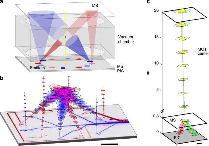
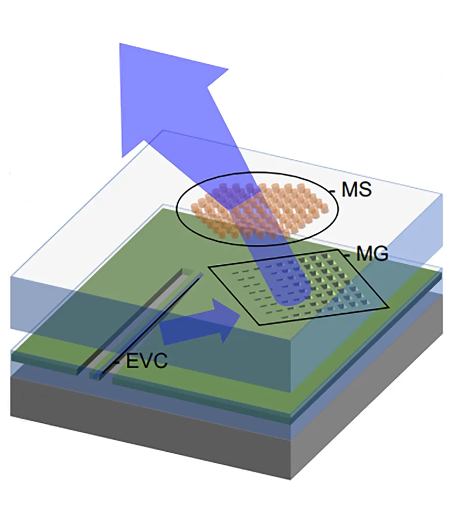
The researchers designed and fabricated the integrated photonics package using a bonded planar platform that seamlessly merges optical metasurfaces with grating outcouplers. This combination allows the generation of beams with high numerical aperture, arbitrary tilt angles, prescribed polarizations, and collinear propagation. The result is a compact photonic chip system capable of producing twelve circularly polarized beams as large as 10 mm in diameter.
This system has been designed to form both the 461 nm and 689 nm magneto-optical traps (MOTs) within a small volume, accommodating a vacuum chamber with strontium vapor. Additionally, the researchers demonstrated the collinear combination of two separately waveguided beams to produce an optical lattice aligned with a probe beam at the clock transition. The combined lattice and clock beams are collinear to within 0.1° of one another and are vertically directed to within 1° from the chip normal.
One of the key advantages of the integrated photonic platform is its scalability, offering the ability to create an arbitrary number of beams, each with distinct wavelengths, geometries, and polarizations. This flexibility and versatility open up new possibilities for the development and integration of atomic technologies with improved precision and control.
In essence, the integrated photonic chip system represents a significant leap forward in the miniaturization of strontium atomic clocks, paving the way for more advanced and compact atomic technologies that could revolutionize a variety of applications and industries.
Potential Applications and Benefits
The development of the compact photonic chip system for miniaturized strontium atomic clocks has far-reaching implications for various industries and sectors, promising numerous potential applications and benefits:
- GPS Systems: Miniaturized atomic clocks could lead to more accurate and reliable GPS systems, ensuring better navigation and positioning capabilities for consumers, businesses, and the military. With increased precision, new applications could emerge, such as highly automated transportation systems, precision agriculture, and advanced surveying technologies.
- Communication Networks: In telecommunications, highly accurate atomic clocks are essential for synchronizing data transmission and managing traffic in networks. The integration of miniaturized atomic clocks could lead to improvements in communication networks’ performance, stability, and efficiency, benefiting both consumers and businesses.
- Aerospace and Defense: The development of compact atomic clocks can significantly impact aerospace and defense industries, where highly accurate timekeeping is crucial for satellite-based applications, missile guidance systems, and secure communication channels. The miniaturization of atomic clocks could lead to lighter, more efficient, and cost-effective systems.
- Scientific Research: Miniaturized atomic clocks could greatly benefit scientific research in fields such as physics, astronomy, and geoscience, where highly precise timekeeping is required. The reduced size and complexity of these optical systems could enable new experimental setups and facilitate the development of novel research tools.
- Financial Markets: High-frequency trading and other financial transactions rely on highly accurate timekeeping to maintain fairness and transparency in global financial markets. The integration of miniaturized atomic clocks in financial systems could enhance the precision and integrity of transactions, ensuring a more stable and secure global financial infrastructure.
- Internet of Things (IoT) and Edge Computing: As IoT devices and edge computing systems become increasingly prevalent, the need for accurate and reliable timekeeping grows. Miniaturized atomic clocks could be integrated into IoT devices and edge computing systems, providing precise synchronization and enabling advanced applications, such as smart cities and industrial automation.
By revolutionizing atomic technologies through miniaturization, the compact photonic chip system offers a wealth of potential applications and benefits across a diverse range of industries. The increased precision, reduced size, and enhanced accessibility of these optical systems open up new possibilities for innovation and advancement in various sectors.
Future Developments and Research Directions
As this groundbreaking research continues, there is potential for further improvements to the photonic chip system. The integration of this technology with other atomic technologies could lead to even more advanced and precise devices. Moreover, the potential for commercialization and mass production of these miniaturized atomic clocks could revolutionize industries that rely on accurate timekeeping and navigation.
The development of a compact photonic chip system for miniaturized strontium atomic clocks marks a significant advancement in the field of atomic technologies. This research has the potential to impact a wide range of applications, from GPS systems to communication networks. As researchers continue to explore the possibilities of this innovative technology, the future looks promising for the miniaturization of atomic clocks and their integration into various industries.