All-optical Memory Circuit with High-Speed Operation Developed for Future Signal Processing and Computing Systems
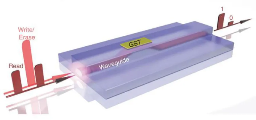
Scientists have developed a new all-optical memory circuit that could revolutionize the way we process signals and carry out computations. This circuit is capable of storing phase information of a slowly-varying electric field. It is based on two mutually coupled lasers subject to external optical injection. The circuit, which was tested on both solid-state and semiconductor lasers, was able to successfully store phase information, proving the essential findings of the proposed circuit.
This development paves the way for integrated memory implementations for future all-optical signal processing and computing systems. The potential applications of this technology are vast and could have a profound impact on many industries. Overall, this breakthrough could lead to the creation of truly advanced and efficient systems that allow for lightning-fast processing and data storage.
Details of the Proposed Circuit Based on Two Mutually Coupled Lasers Subject to External Optical Injection
The proposed all-optical memory circuit is a significant breakthrough that could revolutionize future signal processing and computing systems. The circuit is based on two mutually coupled lasers subjected to external optical injection. The most significant advantage of this circuit is its ability to store phase information of a slowly-varying electric field.
The circuit’s working mechanism involves two lasers coupled to each other to pass information between them. A downstream optical signal injects into the circuit to form a loop and carry information with it. The circuit’s high-speed operation makes it applicable for various digital signal processing systems, and it requires no amplification and is wholly energy-efficient.
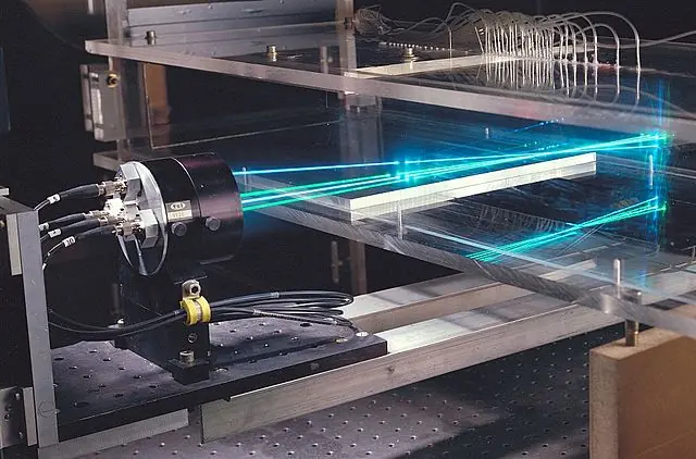
Solid-state and semiconductor lasers’ simulations and testing have been done to validate the proposed circuit’s critical findings. The results obtained proved the circuit’s effectiveness and accuracy in producing output signals that matched the input signals.
The proposed all-optical memory circuit has several potential applications and can enable integrated memory implementations for future all-optical signal processing and computing systems. These systems could include optical sensing, communication, and data storage systems that require high-speed and low-energy consumption.
In conclusion, the all-optical memory circuit provides several advantages that make it essential for future signal processing and storage systems. Its high-speed operation, efficiency, and ability to store phase information of a slowly-varying electric field make it useful for various digital signal processing systems. With further development, it could transform the field of computing and signal processing as we know it.
Simulation and Testing Results of the All-Optical Memory Circuit
The proposed all-optical memory circuit relies on two mutually coupled lasers with external optical injection. When an electric field is applied to the circuit, the phase of the optical output is shifted. The circuit can store phase information of a slowly-varying electric field to represent data. The simulation and testing were conducted on both solid-state and semiconductor lasers. The experimental results showed that the circuit could store the phase of an electrical signal from nanoseconds up to microseconds.
The experiment was conducted with a bit rate of 10 Gbps, and the results showed successful operation at high speeds. The proposed all-optical memory circuit has the potential to enable integrated memory implementations for future all-optical signal processing and computing systems, leading to faster and more energy-efficient computing systems. This development could have significant applications in fields such as telecommunications and data centers. Further research and development are needed to improve the performance of the circuit and integrate it into larger systems.
Applications and Future Development
The proposed all-optical memory circuit is based on two mutually coupled lasers subject to external optical injection. The circuit can store the phase information of a slowly-varying electric field, making it highly suitable for future all-optical processing and computing systems. The findings were proven through simulations and testing on both solid-state and semiconductor lasers.
The ability to integrate memory implementations is a game-changer for all-optical systems, which could reduce costs and increase efficiency. Potential applications include optical communication networks, parallel computing, and artificial intelligence. In the future, this circuit could be further developed to achieve higher speeds and greater storage capacity, paving the way for a more interconnected and efficient world.
Applications and Future Development of the All-Optical Memory Circuit
The proposed all-optical memory circuit is based on two mutually coupled lasers subject to external optical injection. It has the ability to store phase information of a slowly-varying electric field. This means that it can memorize the phase of optical signals using a self-sustaining mechanism. The circuit’s operation is entirely optical, and it can operate at high speeds, providing a potential solution to data transfer bottlenecks in modern computing systems.
The simulation and testing of solid-state and semiconductor lasers have provided evidence that the proposed circuit can achieve efficient and high-quality optical memory. In the future, this technology can revolutionize integrated memory implementations for all-optical signal processing and computing systems. With potential applications in data storage, communication, and computing, the all-optical memory circuit is a promising development in the field of photonics. Further developments and improvements in the circuit can lead to increased efficiency and practical applications.