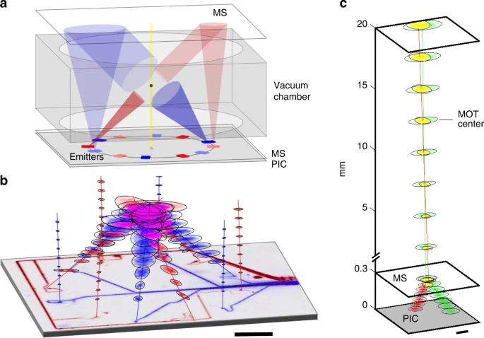
a The photonics geometry as part of the strontium clock, showing the four types of beams including a pair of the red and blue beams at 0° (light color) and 45° (dark color), as well as the collinearly combined lattice and clock beams (yellow). b Measured trajectories of the twelve blue and red MOT beams, overlayed on an image of the PIC. Scale bar is 5 mm. c Measured trajectories of the lattice (green) and clock (red) beams below and above the MS (yellow region depicts the overlap of the two beams). Scale bar is 100 µm

Compact Photonic Chip System Brings Miniaturized Atomic Clocks Closer to Reality

Researchers have developed a groundbreaking compact photonic chip system that paves the way for miniaturized strontium atomic clocks. The achievement has significant implications for atomic technologies, as miniaturization could lead to a range of benefits in applications such as GPS and communication systems.

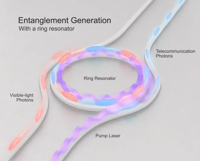
By carefully engineering the geometry of a micrometer-scale, ring-shaped optical resonator, researchers at NIST produced pairs of entangled photons (particles of light) that have two very different colors or wavelengths. Light from a pump laser (purple regions in the resonator) generates one photon in each pair at a visible-light wavelength (red patches in and around resonator); the other photon has a wavelength in the telecommunications (near-infrared) part of the spectrum (blue patches). From the perspective of quantum communication, these pairings combine the best of both worlds in an optical circuit: The visible-light partner can interact with trapped atoms, ions, or other systems that serve as quantum versions of computer memory, while the telecommunications wavelength member of each couple is free to propagate over long distances through an optical fiber network. Credit: S. Kelley/NIST

Optical Resonators: Principles, Types, and Applications in Modern Technology

Optical resonators, sometimes referred to as optical cavities, are essential components in various modern technologies, from lasers and optical sensors to telecommunications systems. By trapping and circulating light within a defined space, these devices can amplify or manipulate light waves, resulting in a wide array of practical applications.

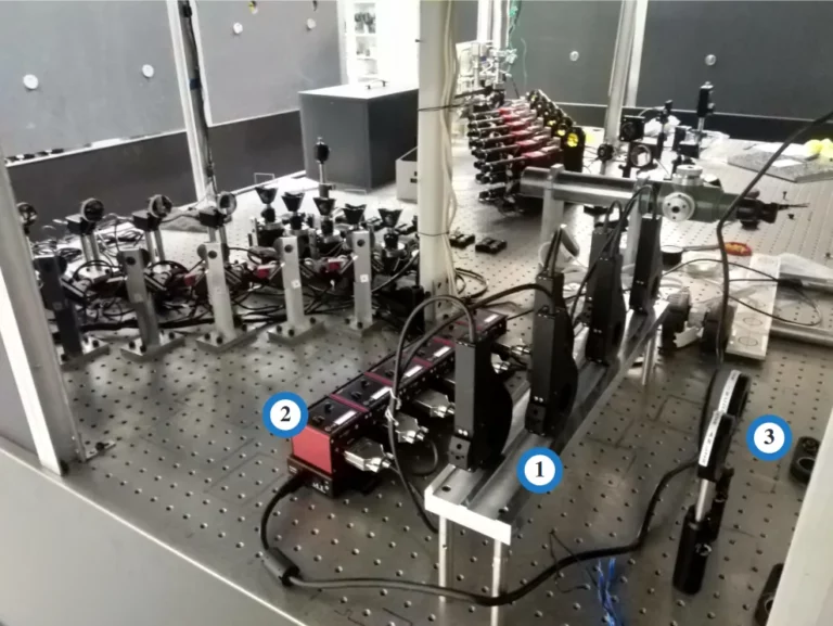
The new polarimetric hardware installed on the MIRC-X optical bench at CHARA. The top panel shows the Air Spaced Waveplates assembly (1) and motor control boxes (2) in relation to the MIRC-X instrument during initial testing in 2019 November, where calibration was conducted with a pair of linear polarizers (3).

Understanding Air Spaced Waveplates: Applications and Principles

The field of optics has seen significant advancements in recent years, and one of the essential components driving these innovations is the air spaced waveplate. This article aims to provide a comprehensive understanding of air spaced waveplates, their principles, applications, and how they differ from other waveplates.

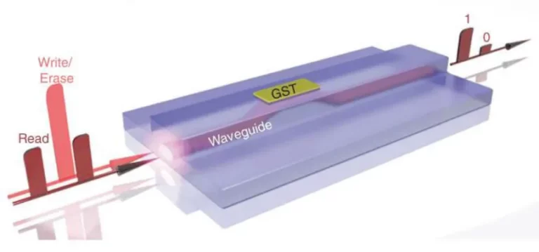
Schematic of an optical photonic-memory cell.

All-optical Memory Circuit with High-Speed Operation Developed for Future Signal Processing and Computing Systems

Scientists have developed a new all-optical memory circuit that could revolutionize the way we process signals and carry out computations. This circuit is capable of storing phase information of a slowly-varying electric field. It is based on two mutually coupled lasers subject to external optical injection.

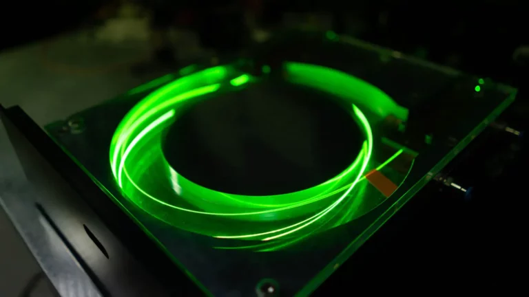
Injection of a Helium-Neon laser beam into a plastic optical fiber.

Yttrium-Aluminum-Garnet Crystal-Derived Silica Fiber Laser Boasts Over 60% Optical-to-optical Conversion Efficiency

Researchers have successfully fabricated a silica optical fiber derived from yttrium-aluminum-garnet (YAG) crystals, demonstrating superior output power and optical-to-optical conversion efficiency in linearly polarized single-frequency fiber lasers (LPSFFLs).

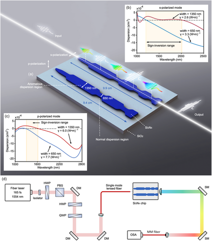
Ultraefficient on-Chip Supercontinuum Generation from Sign-Alternating-Dispersion Waveguides.

A Quantum Leap in Efficiency: 3 Orders of Magnitude Improvement in On-Chip Supercontinuum Generation

Researchers have achieved a groundbreaking advancement in the field of ultraefficient on-chip supercontinuum generation, paving the way for the development of portable and mechanically stable medical imaging devices, chemical sensors, and light detection and ranging (LiDAR) systems.

End of content

End of content