The Emergence of Multiphoton Lithography in the World of Micro-Optics
The field of micro-optics is rapidly growing and essential advancements are being made in multi-photon laser lithography (MPL) for 3D printing. MPL, also known as two-photon or multi-photon polymerization, is a game-changing technology that is attracting increasing industrial interest from key established companies in the field. This review will detail the origin and advancement of micro-optics fabrication with MPL by describing the chronology, distinguishing discrete application groups, providing generalized technical data on the processes and available materials, and discussing the foreseen near-future advances.
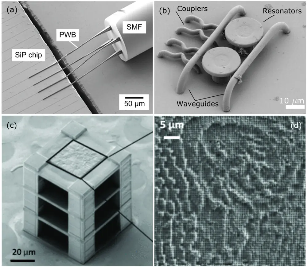
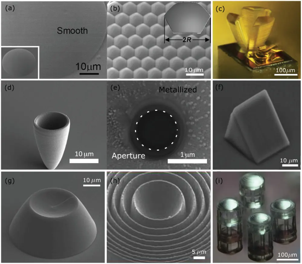
The rapid growth of laser applications has increased the demand for new optical components, and devices are becoming miniaturized and highly integrated to maximize functionality. MPL is a result of the intersection between the fields of laser technology and industrial trends. The first use of ultrafast lasers for 3D structuring was proposed in 1991 for optical data storage, and it was first presented as a tool for creating 3D printed objects in 1997. However, it took some time for the technology to mature from proof-of-principle level to a reliable additive manufacturing tool for efficient fabrication in modern labs. By 2020, MPL was already an established technique for routine fabrication of diverse micro-optical single elements, stacked components, and integrated devices. The latest advances in 3D printing of free-form micro-optics are enabled by optical grade materials of high refractive index polymers, high-performance hybrids, and optically active or pure inorganic glasses.
The advances in this field have attracted the attention of the related laser-assisted precision additive manufacturing industry, leading to the establishment of several companies oriented towards commercialization of this technology. There are now a number of MPL commercial setups specifically for micro-optics, and advances are expected in establishing advanced metrology dedicated for 3D micro-optics and standardizing the protocols for comparison and repeatability.
Since its emergence 25 years ago, the field of micro-optics has been rapidly expanding and is still the most versatile technique for designing, creating, and testing novel materials. MPL is a unique tool for complex free-form geometries for 3D micro-optics and provides a higher-throughput and wider variety of architectures, especially photonic integrated circuits. Most recent advances in active optical compounds, high refractive index, and high resilience substances enable the additive manufacturing of heavy-duty microdevices that are compatible with current existing platforms.
In conclusion, MPL is a rapidly expanding field that has already established itself as a versatile and reliable tool for routine fabrication of diverse micro-optical elements and integrated devices. The field is expected to continue to grow, with further advances in metrology, standardization, and the integration of heavy-duty materials into established platforms. MPL is poised to revolutionize the field of micro-optics and bring new possibilities to a wide range of applications.